Running Design Rule Checks in KiCad
How to ensure a PCB layout can be manufactured without issue
Why run Design Rule Checks?
When designing a printed circuit board it is crucial to use sensible design rules to ensure that the layout of the board is manufacturable. Common manufacturability errors are traces which are too small or too closer together, as well as via sizing and spacing which is not achievable through normal manufacturing methods. This blog will show how to set up design rules in KiCad so that a design rule check can be performed before the design is uploaded to the FlashPCB upload portal.
How to setup DRC in KiCad
There are two primary methods for setting up design rules in KiCad: importing settings from another board, or entering all values manually. Importing rules from an existing board will be covered first.
I. Import KiCad Design Rules Step-by-Step
1. Download Existing Design File
In order to import board settings from another board, it is recommended to download KiCad DRC File as it contains FlashPCB manufacturing constraints.
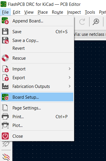
2. Open Board Setup
Next, open the .kicad_pcb file which will have the design rule checks run and navigate to File>Board Setup.... This is where PCB setup information and design contraint information is established within KiCad.
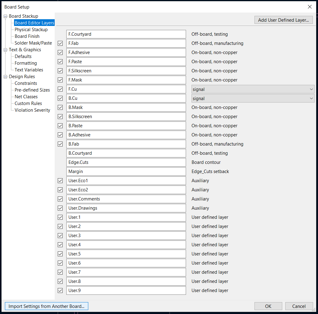
3. Import Existing Rules Set
Click “Import Settings from Another Board…” at the bottom of the Board Setup pop-up.
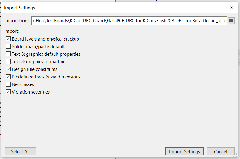
4. Select Existing KiCad DRC from Another Board File
Navigate to the previously downloaded file “FlashPCB DRC for KiCad.kicad_pcb” file. Once the file is selected check the following boxes to ensure that the most important design rules are imported to this current design: "Board layers and physical stackup, Design rule constraints, Predefined track & via dimensions, Violation Severities". The other check box options are not necessary as they will not affect the physical PCB functionality. Keep in mind that silkscreen text smaller than 0.1mm text thickness is generally not manufacturable.
5. Close Pop-ups and Review Rules
Once the appropriate import selections have been made, click “Import Settings” to close the Import Settings pop-up. Then click “OK” to close the Board Setup pop-up.
II. Establish KiCad Design Rules Manually
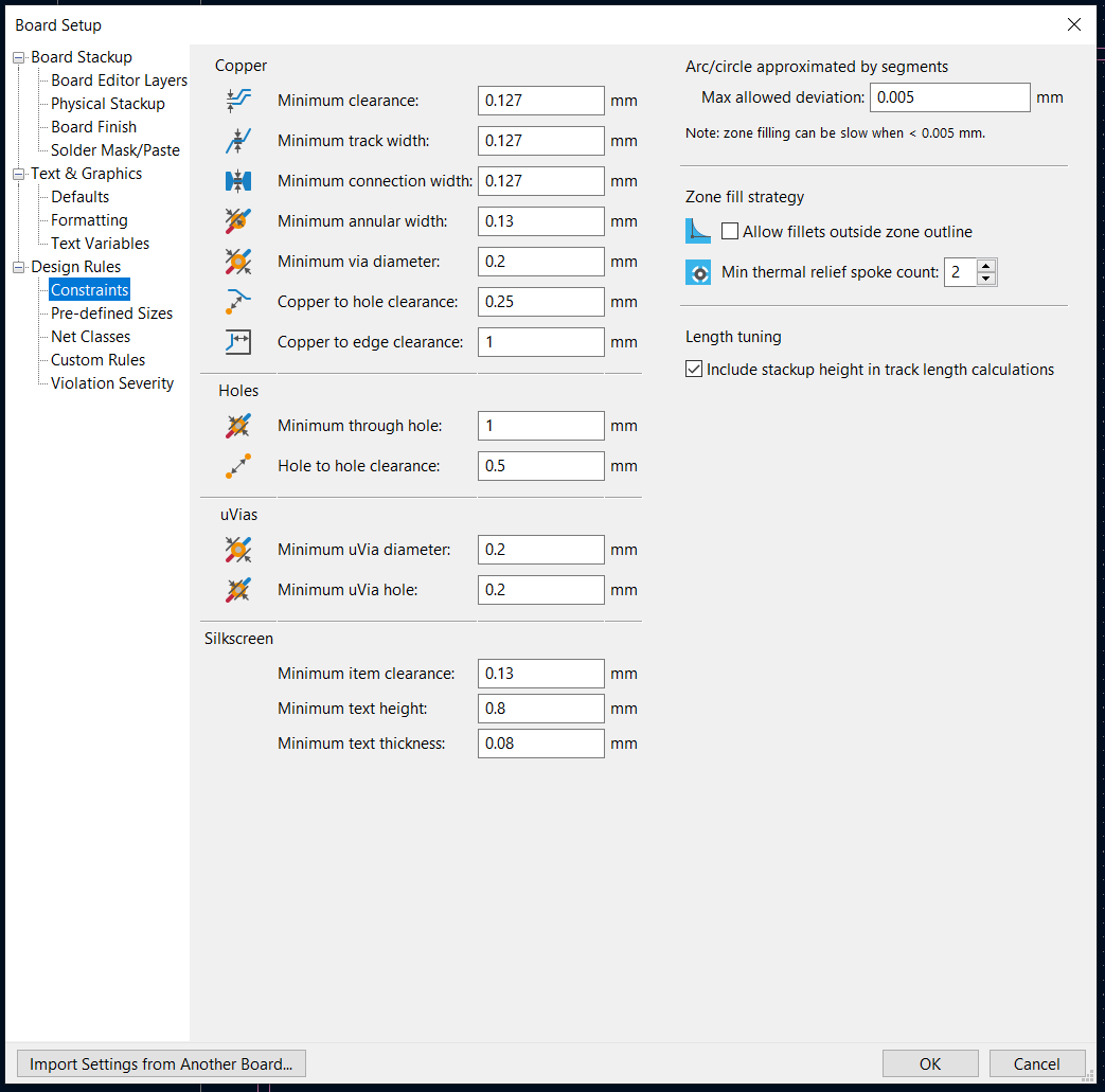
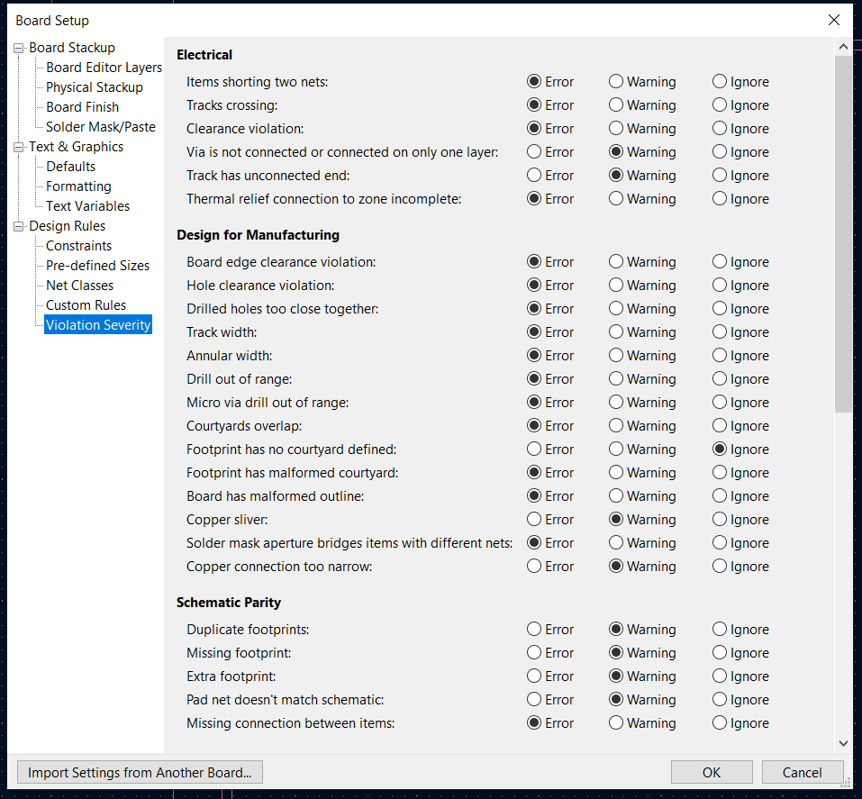
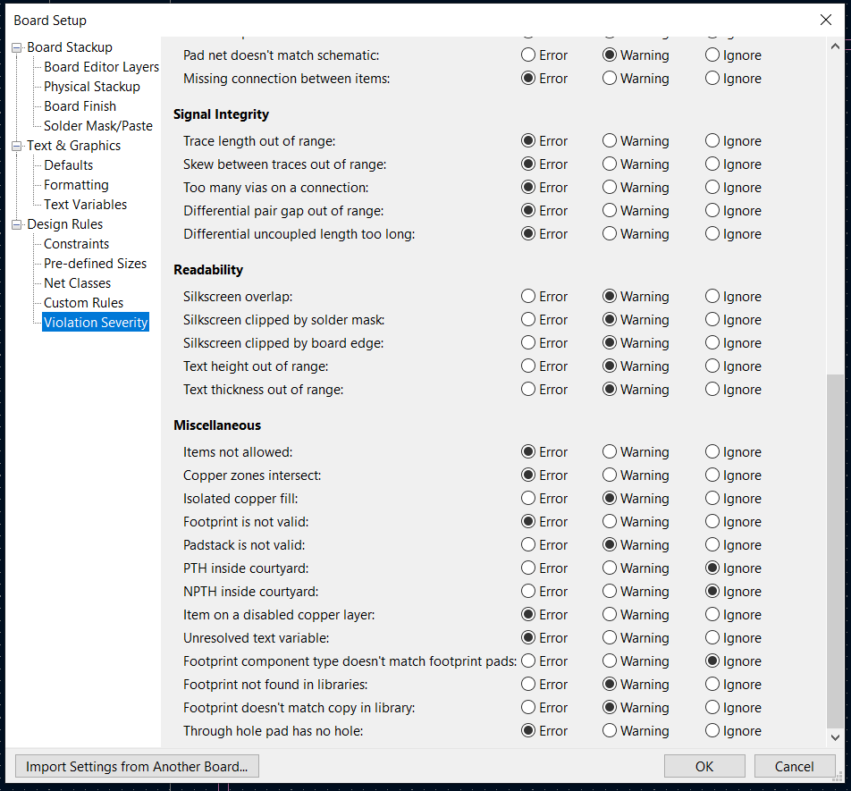
It is also possible to simply enter in all the relevant design rule information manually. While this method is more time consuming it is just as effective. Use the values from the images below to ensure the design is manufacturable within FlashPCB design limitations:
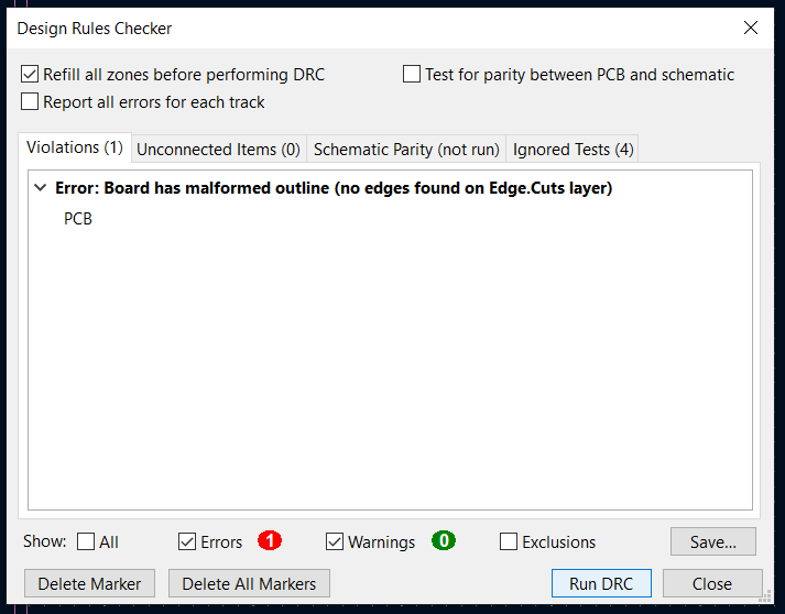
III. Perform Design Rule Check to Verify Layout
Once the design rules have been established within KiCad, at the top row find the function “Show design rules checker window”. Once the Design Rules Checker GUI appears, click “Run DRC” and wait as the design is compared against the previously set rules. Any design errors which appear should be rectified before attempting to upload to the FlashPCB portal.