The Rise of Wafer Level Chip Scale Packages (WLCSP)
Exploring the Evolution, Efficiency, and Impact of WLCSP in Modern Semiconductor Technology
This is the fourth blog post in our series about the miniaturization of IC packages. In Part 1, we provided an overview of the four common IC packages: Quad Flat Package (QFP), Quad Flat No Lead (QFN), Ball Grid Array (BGA), and Wafer Level Chip Scale Packaging (WLCSP). In Part 2, we examined the transition from QFP to QFN, analyzing 44 unique QFP packages and 35 unique QFN packages to explore the theoretical limits of contact densities. In Part 3, we focused on the transition to BGA, analyzing 105 unique BGA packages. We used the theoretical limits of contact density to illustrate why this shift was necessary as ICs became smaller and more complex. In our Part 5 we share all the data we collected in this blog series.
Wafer Level Chip Scale Packages
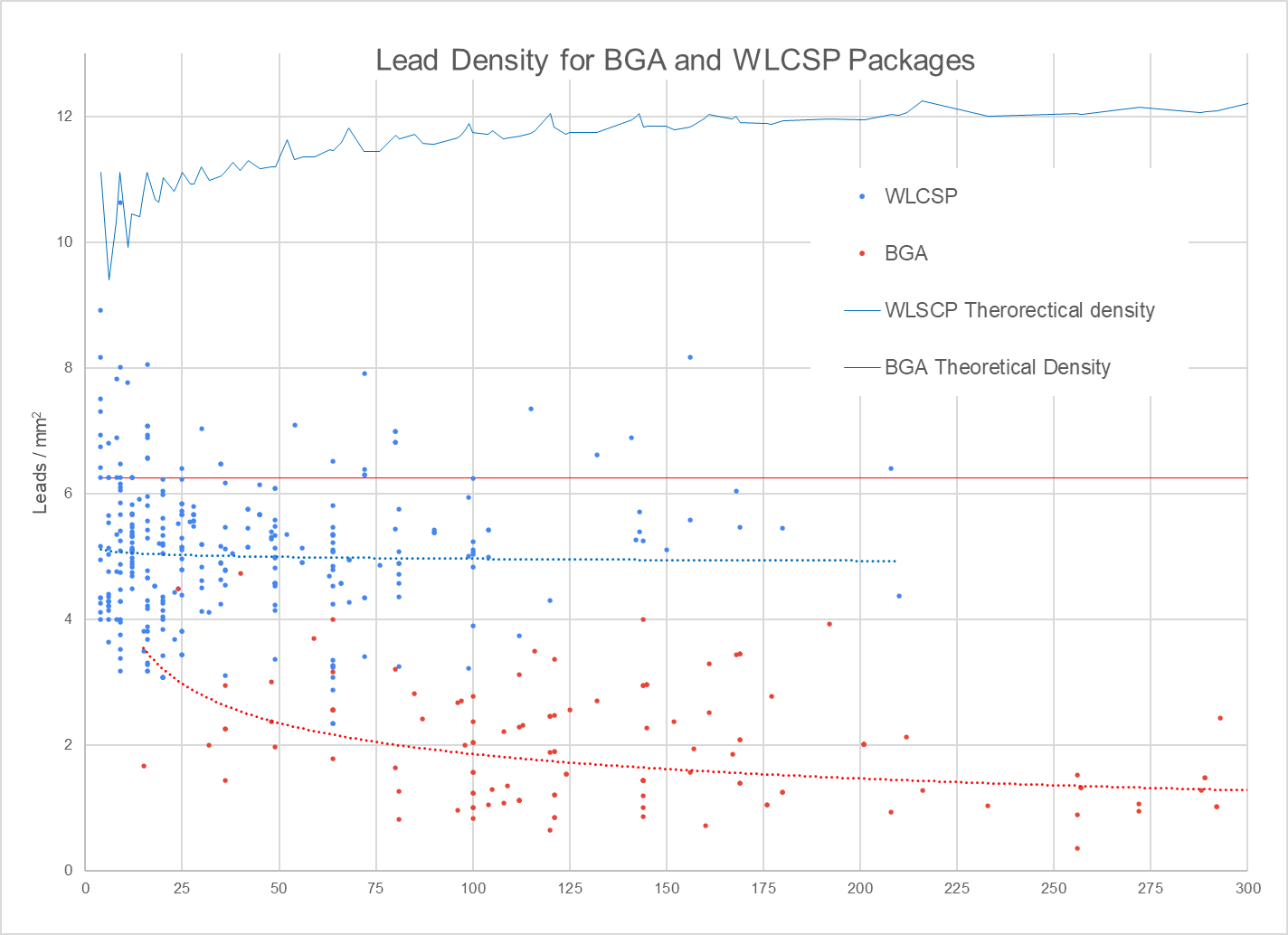
As we saw in our analysis of pin density, the space efficiency of BGAs is only dependent on the pitch of the packages. Wafer Level Chip Scale Packages (WLCSP) were developed to meet the industry's needs for smaller, faster, more reliable, and cost-effective semiconductor packages by reducing the pitch below 0.4mm.
WLCSP can reduce pitches below 0.4mm by eliminating the need for a separate substrate between the silicon die and the ball grid array. In traditional BGAs, the bottom of the package is a laminate substrate with the solder balls mounted. The silicon die is then mounted to the substrate with wire bonding or a direct mount using “flip chip” methods.
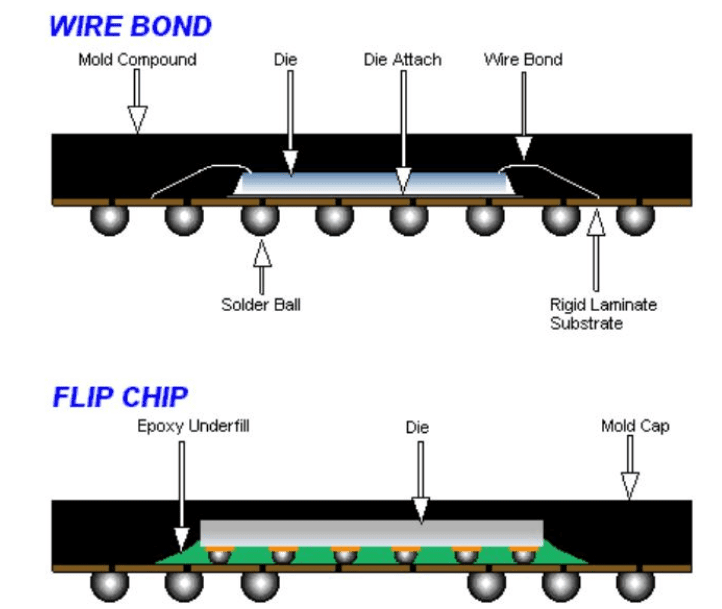
By eliminating the substrate, WLCSP reduces the parasitic inductance and capacitance associated with traditional BGA packaging methods. This leads to better electrical performance, faster signal transmission, and improved overall device performance. By integrating the packaging process directly at the wafer level, WLCSP reduces the number of assembly steps, leading to lower manufacturing costs and offering better reliability. It also simplifies the supply chain and reduces material usage, contributing to cost efficiency.
Package Data
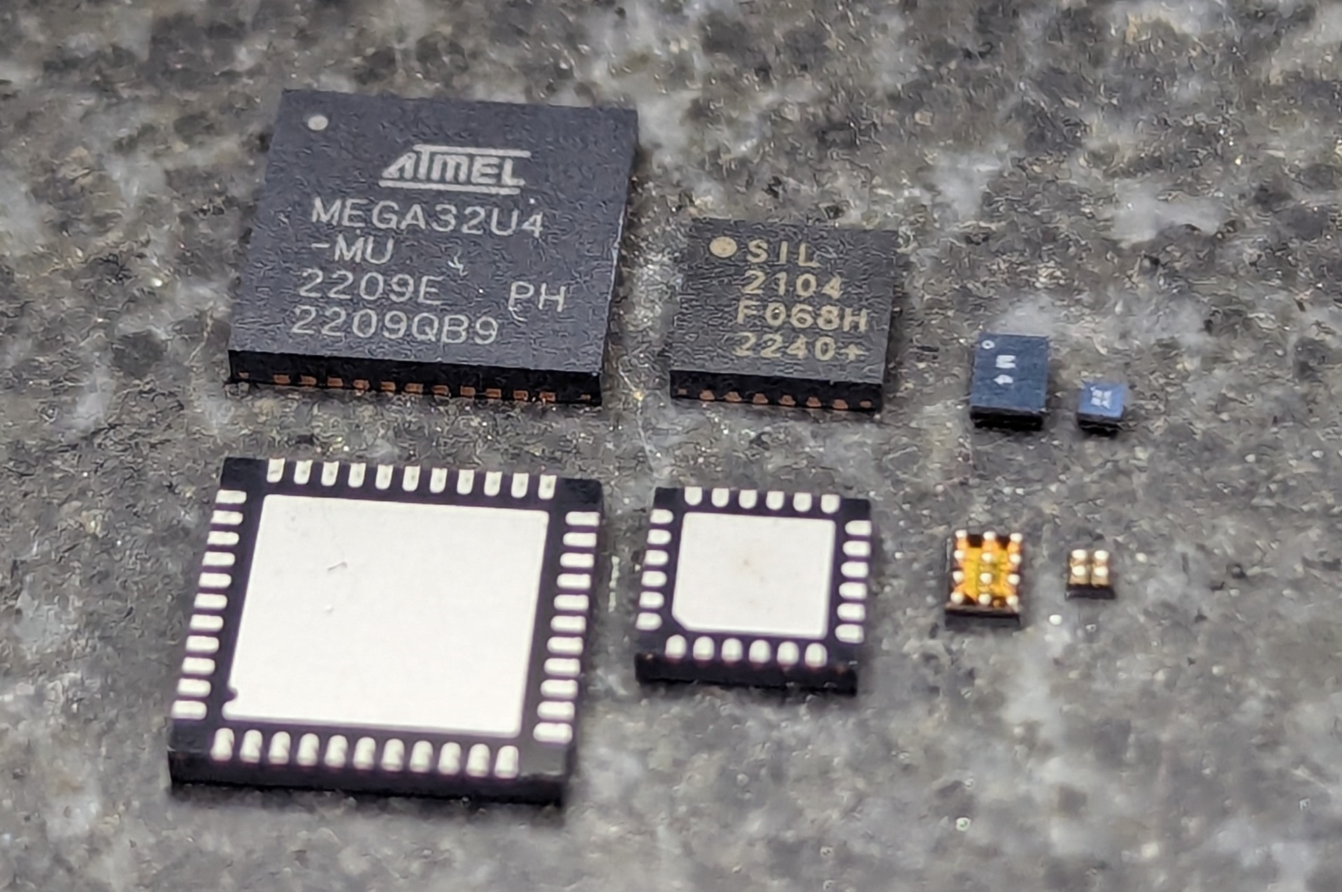
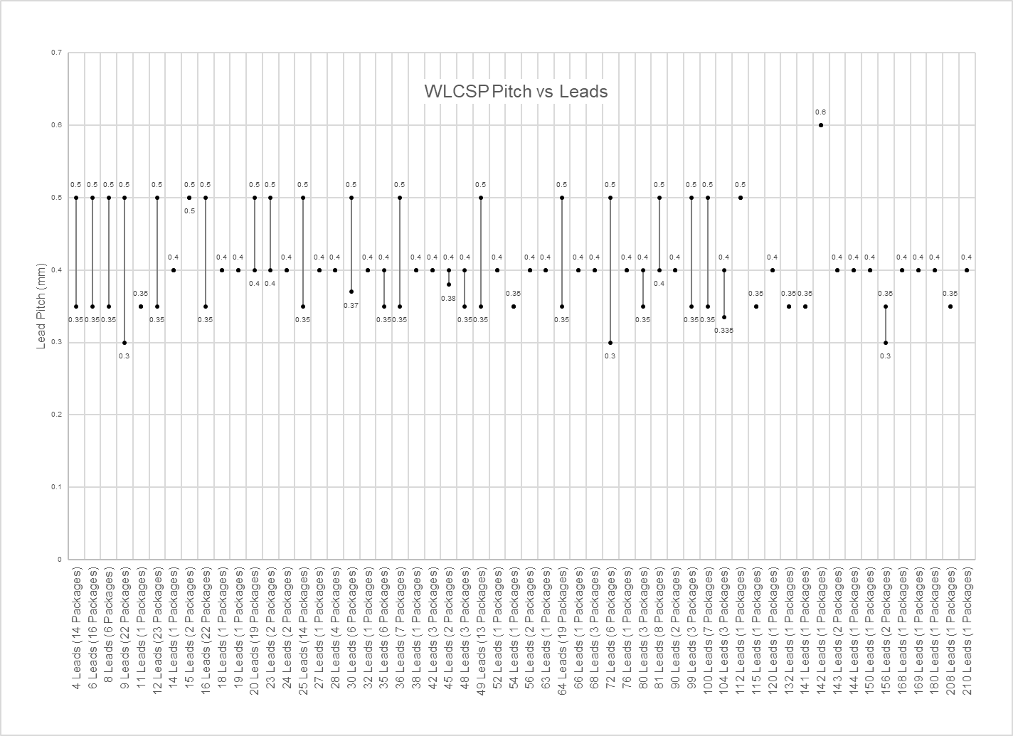
We compiled data on 271 unique WLCSP packages for this analysis. These packages were identified through queries of Digi-Key’s inventory of components filtered by the supplier package. There is a vast array of package dimensions because the package is formed directly from the wafer and not in a molding process. These dimensions no longer fall in whole numbers and square packages, as wafer space is very expensive and each component is made to minimize wafer size. So, while a BGA package would typically be 7.0mm by 7.0mm, a WLCSP would be 2.8819mm by 3.1024mm.
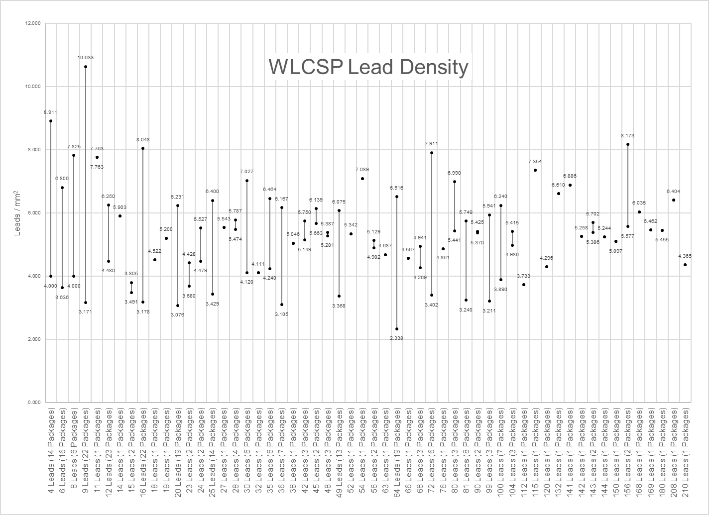
Most pitches for WLCSP were 0.5mm or smaller, with only one package having a 0.6mm pitch. The smallest pitch in our dataset was 0.3mm.
Max Theoretical Lead Density
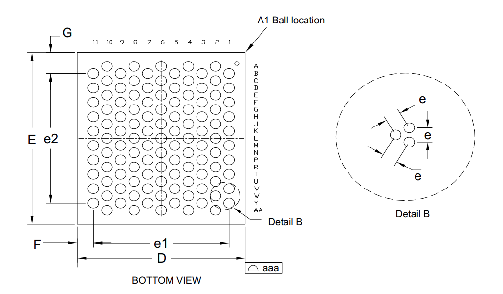
The max theoretical lead density for a WLCSP is derived from the pitch. However, unlike most BGAs that have a rectangular grid, many WLCSPs use a hexagonal packing arrangement. We can see this really well in the STM32H725AG MCU from STMicroelectronics.
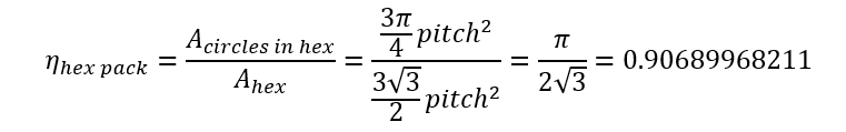
We can calculate the theoretical maximum lead density by looking at the packing density of circles in a hexagonal arrangement:
.png)
The diameter of the circle, in this case, is the pitch and is equivalent to the side length of the hexagon. We can then calculate the packing efficiency:
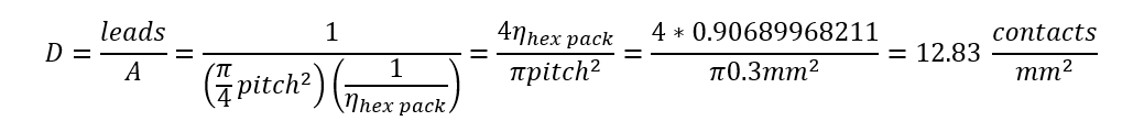
From this, we can calculate contact density from the area each contact requires. The smallest pitch in our sample of 271 WLCSPs was 0.3mm, so the max theoretical contact density is:
However, this does not account for the edge cases and only considers continuous sections of hexagonally packed circles, where square packing is optimal for 4, 9, 16, 25, and 36. Fortunately, Dr. Eckehard Specht has compiled a list of optimal packing for circles in a square for up to 10,000 circles. This data is compiled here.
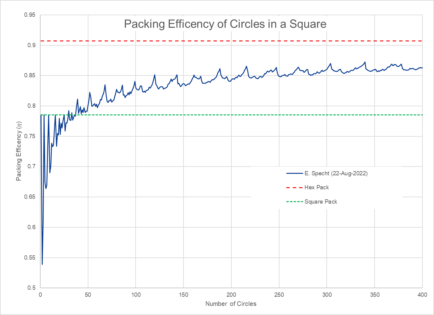
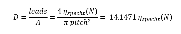
With this, we can recalculate the maximum contact density as a function of the number of leads using the Specht packing efficiency data as a lookup table:
Conclusion
The evolution of IC packaging from QFP to QFN, BGA, and ultimately to WLCSP highlights the industry's relentless pursuit of miniaturization, performance enhancement, and cost efficiency. WLCSP is the current lead edge technology, offering superior electrical performance, reduced parasitic effects, and a streamlined manufacturing process.
Get More Information
Part 1: Miniaturization of IC Packages
Part 2: Exploring IC Package Miniaturization: QFP and QFN
Part 3: The move from QFN and QFP to Ball Grid Array
Part 5: All the IC Package Data in One Place: QFP, QFN, BGA, and WLCSP
For more information sign up at here.